KNX: Unterschied zwischen den Versionen
Thoto (Diskussion | Beiträge) |
Thoto (Diskussion | Beiträge) (→Results) |
||
| (12 dazwischenliegende Versionen von 2 Benutzern werden nicht angezeigt) | |||
| Zeile 4: | Zeile 4: | ||
|image = | |image = | ||
|description = KNX implementierung | |description = KNX implementierung | ||
| − | |author = mat, | + | |author = mat, [[User:thoto|Endres]], [[User:thoto|thoto]] |
| − | | | + | |
|version = | |version = | ||
|update = | |update = | ||
| Zeile 12: | Zeile 11: | ||
|download = https://devtal.de/knx/knx.git/ | |download = https://devtal.de/knx/knx.git/ | ||
}} | }} | ||
| + | == Prototype board == | ||
| + | <gallery> | ||
| + | File:Knx-board-1.jpg|prototype KNX transciever board: bottom | ||
| + | File:Knx-board-2.jpg|prototype KNX transciever board: top | ||
| + | </gallery> | ||
| − | + | A KNX bus terminal block can be plugged in on the top of the board by the two contacts on the left side. The pin header on the other side provides a digital interface to be connected to a microcontroller and terminals to utilize the bus powering feature of KNX. | |
| − | == MOSFET based transmitter | + | == MOSFET based transmitter circuit == |
| − | + | [[File:Knx-mosfet.jpg|thumb|right|MOSFET sender realization]] | |
| − | + | === Introduction === | |
| + | The simulation shows the basic characteristics of the MOSFET based transmitter circuit compared to the original BCP52 PNP-BJT based one. We wanted to evaluate this because we wanted to play around with MOSFETs a bit and lower the price and heat dissipation of the transmitter. Therefore the circuit is quite hacked together and also shows some bad behavior: | ||
| + | * the circuit drains around 6mA of current to ground when the voltage spikes generated by the inductance reach its peak value -- even if the signal is not generated by the MOSFET itself but by another transmitter | ||
| + | * there is a short dip in voltage just at the beginning of the pulse. It is inside tolerance declared by the specification. | ||
| + | * we did not evaluate behavior of parts due to manufacturing tolerances and over temperature range but expect bad results. (Quick simulations of the circuit at different temperatures show that it does its job quite well from -20°C to 80°C.) | ||
| + | * it does not match the requirements in EN 50090-5-2:2004 pp. 40 since t_active is longer than 35us. That is mainly due to the low voltage drop from the gate. This may be fixed in software. | ||
| − | === | + | There are measurements inside the simulation verifying the characteristics against the parameters in the specification. |
| + | |||
| + | === Description of parts in MOSFET circuit === | ||
| + | |||
| + | <!-- | ||
| + | * D1 and D2 ensure that the bus and supply voltage are always positive in the circuit. | ||
| + | * R6 and R7 are used for current measurements in simulation. | ||
| + | * D3 establishes a potential of V_bus-3.9V at the gate of M1. Therefore the potential at the FET gate is adjusted to just below U_th and the (very small) initial current into the gate is reduced which improves the switching behaviour. Without D3 there would be a dip in V_bus when M1 is switched on. | ||
| + | * D4 generates a voltage of Vconst - 10V - U_R2 at the gate of the FET. The FET has U_th \in [-2,-4] V, so in average 6.3V voltage drop with respect to Vbus are generated (also notice U_D1 and U_D2!) when triggering M1. | ||
| + | --> | ||
* D1 und D2 sorgen dafür, dass die Spannung am Bus und die Versorgungspannung immer positiv sind. | * D1 und D2 sorgen dafür, dass die Spannung am Bus und die Versorgungspannung immer positiv sind. | ||
| Zeile 31: | Zeile 49: | ||
* R1 ist eine Sicherung. Praktisch zum Strom messen. | * R1 ist eine Sicherung. Praktisch zum Strom messen. | ||
* R4 stellt das Basispotential von Q1 ein, R5 begrenzt den Basisstrom. C1 entkoppelt Q1, sodass eine kontinuierliches Spannung nur ein temporäres Durchsteuern von Q1 erzeugen kann. | * R4 stellt das Basispotential von Q1 ein, R5 begrenzt den Basisstrom. C1 entkoppelt Q1, sodass eine kontinuierliches Spannung nur ein temporäres Durchsteuern von Q1 erzeugen kann. | ||
| + | |||
| + | === Software Requirements === | ||
| + | To run the simulation you should use at least KiCAD 5.0.0rc2 with SPICE simulation enabled and ngspice-28. It may be possible to generate a netlist and use ngspice manually, but this is not tested yet. | ||
| + | |||
| + | Note on Debian support: The SPICE simulation part of KiCAD 5 is explicitly disabled in the official Debian unstable/sid KiCAD packages at the moment (2018-06-14). You need to modify both the ngspice and KiCAD packages and build them yourselves to enable building ''libngspice.so'' and enable the use of libngspice in KiCAD. If these changes should not be included in the official packages in the near future, we will release build instructions and maybe a Docker image to simplify installation. In the meantime you could try building it yourself. | ||
| + | |||
| + | If you are using Arch Linux you can use the official ngspice package, which includes the shared library support and build the AUR kicad-git package for KiCAD 5 as long as it isn't officially released. | ||
| + | |||
| + | If you have any issues building or need instructions right now just write a short mail to [[User:thoto|thoto]]. | ||
| + | |||
| + | === Results === | ||
| + | The simulation contains measurements of the time t_active of a pulse according to DIN EN 50090-5-2 section 5.2 and the according voltage levels on the bus. The plot of the transient simulation below shows the bus voltage (green coloured graph) when | ||
| + | * 35µs .. 70µs: the MOSFET circuit generates a "0"-pulse | ||
| + | * 218us .. 251µs: the BJT circuit generates a "0"-pulse | ||
| + | * 416µs .. 451µs: both generate a pulse at the same time | ||
| + | |||
| + | Simultaneously the current through resistor R1 is measured (red graph) which indicates the times the MOSFET is activated. At t=250µs there is an unwanted current due to the high voltage peak of the power compensation pulse on the bus. The long current fall time is visible as well. | ||
| + | [[File:Knx-mosfet-sim1.png|thumb|center|600px|axis labels to be added soon ... Y axis: current: -1..23mA (lines on right side), voltage: 22..56V (grid, left side); X axis: 0..700us, 50us grid size]] | ||
Aktuelle Version vom 22. September 2018, 00:18 Uhr
| KanNiX Release status: experimental [box doku] | |
|---|---|
| Description | KNX implementierung |
| Author(s) | mat, Endres, thoto |
| Platform | diskrete Bauelemente und Mikrocontroller |
| License | GPLv3 |
| Download | https://devtal.de/knx/knx.git/ |
Inhaltsverzeichnis
Prototype board
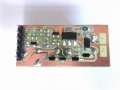
prototype KNX transciever board: bottom
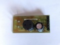
prototype KNX transciever board: top


A KNX bus terminal block can be plugged in on the top of the board by the two contacts on the left side. The pin header on the other side provides a digital interface to be connected to a microcontroller and terminals to utilize the bus powering feature of KNX.
MOSFET based transmitter circuit

Introduction
The simulation shows the basic characteristics of the MOSFET based transmitter circuit compared to the original BCP52 PNP-BJT based one. We wanted to evaluate this because we wanted to play around with MOSFETs a bit and lower the price and heat dissipation of the transmitter. Therefore the circuit is quite hacked together and also shows some bad behavior:
- the circuit drains around 6mA of current to ground when the voltage spikes generated by the inductance reach its peak value -- even if the signal is not generated by the MOSFET itself but by another transmitter
- there is a short dip in voltage just at the beginning of the pulse. It is inside tolerance declared by the specification.
- we did not evaluate behavior of parts due to manufacturing tolerances and over temperature range but expect bad results. (Quick simulations of the circuit at different temperatures show that it does its job quite well from -20°C to 80°C.)
- it does not match the requirements in EN 50090-5-2:2004 pp. 40 since t_active is longer than 35us. That is mainly due to the low voltage drop from the gate. This may be fixed in software.
There are measurements inside the simulation verifying the characteristics against the parameters in the specification.
Description of parts in MOSFET circuit
- D1 und D2 sorgen dafür, dass die Spannung am Bus und die Versorgungspannung immer positiv sind.
- R6 und R7 sind zur Strommessung während der Simulation gedacht.
- D3 sorgt für ein Potential von V_bus-3.9V am Gate von M1. Dadurch wird etwa die U_th am FET-Gate eingestellt und ein (sehr geringer) initialer Strom in das Gate verhindert und somit das Schaltverhalten verbessert. Ohne D3 käme es zu einem Unterschwinger von V_bus beim Durchsteuern von M1.
- D4 sorgt für einen Spannungsabfall von 10V - U_R2 am Gate des FET. Da dieser hat U_th \in [-2,-4] V hat entstehen so im Mittel 6.3V Spannungsabfall an V_bus (U_D1 und U_D2 beachten!).
- R2 korrigiert den Spannungsabfall auf die gewünschten V_knx - 6V. ... entfernt wegen zu geringem Strom (sic) in Gate beim Aufladen der Gatekapazität!
- R3 begrenzt den Strom durch Q1 wie gewohnt, Q1 sorgt für den gewünschten Spannungsabfall, wenn dieser durchsteuert. Ohne Durchsteuern von Q1 liegt am Knoten östlich R2 \phi > U_th an, da kein Strom durch D4 fließt.
- R1 ist eine Sicherung. Praktisch zum Strom messen.
- R4 stellt das Basispotential von Q1 ein, R5 begrenzt den Basisstrom. C1 entkoppelt Q1, sodass eine kontinuierliches Spannung nur ein temporäres Durchsteuern von Q1 erzeugen kann.
Software Requirements
To run the simulation you should use at least KiCAD 5.0.0rc2 with SPICE simulation enabled and ngspice-28. It may be possible to generate a netlist and use ngspice manually, but this is not tested yet.
Note on Debian support: The SPICE simulation part of KiCAD 5 is explicitly disabled in the official Debian unstable/sid KiCAD packages at the moment (2018-06-14). You need to modify both the ngspice and KiCAD packages and build them yourselves to enable building libngspice.so and enable the use of libngspice in KiCAD. If these changes should not be included in the official packages in the near future, we will release build instructions and maybe a Docker image to simplify installation. In the meantime you could try building it yourself.
If you are using Arch Linux you can use the official ngspice package, which includes the shared library support and build the AUR kicad-git package for KiCAD 5 as long as it isn't officially released.
If you have any issues building or need instructions right now just write a short mail to thoto.
Results
The simulation contains measurements of the time t_active of a pulse according to DIN EN 50090-5-2 section 5.2 and the according voltage levels on the bus. The plot of the transient simulation below shows the bus voltage (green coloured graph) when
- 35µs .. 70µs: the MOSFET circuit generates a "0"-pulse
- 218us .. 251µs: the BJT circuit generates a "0"-pulse
- 416µs .. 451µs: both generate a pulse at the same time
Simultaneously the current through resistor R1 is measured (red graph) which indicates the times the MOSFET is activated. At t=250µs there is an unwanted current due to the high voltage peak of the power compensation pulse on the bus. The long current fall time is visible as well.
